Introduction
The aim of the experiment was to determine the electrical parameters of the NMOS and PMOS transistors in a setup that consisted of a 4007 IC-chip consisting of NMOS and PMOS, a power supply, and an oscilloscope. At the start of the experiment, measurements taken on the drain current at the NMOS, voltage on drain-source, and the gate-source were positive, while the base-source voltage was negative. The two GPC-18500 voltage outputs were either + or – with a ground functional voltage. To create a negative voltage, the input power supply is connected to the positive voltage and to the ground. A multimeter measures the drain current at the pins when the positive voltage output is functioning. The base current is kept 0 by varying the source current between 0 and 10V and the drain-source varying between 0 and 10V. The graph of drain current versus voltage on the drain-source and several gate-sources has linear, saturation, and cut off characteristics. In practice, the curve on the graph varies with ideal situations.
CMOS Inverter
In another set up, an inverter was built to test its functionality using PMOS and NMOS. Its functionality was tested by initializing the drain voltage to 5V as follows: Ch1 was connected to the oscilloscope and supplied with power that was kept at 5V. The Oscilloscope was used to correct variations in power. PMOS and CMOS provided functionalities of the input voltage gates. The drain voltage for PMOS was 5V. The source voltage from PMOS and the drain voltage from NMOS were combined to provide the output voltage. The oscilloscope controlled and kept the input voltage between 0V and 5V. Then, Virtuoso oscilloscope designed by Cadence, a software program with an integrated IC, was used to validate the results.The Virtuoso software works using a library of procedures which allow the user to create a test bench schematic to verify standard cells developed using an analog circuit simulator. The virtuoso software was also used to design NOR and NAN gates for PMOS and NMOS (Ellersick,11). During the design of the NOR and NAND gates, NAND gates responded equally to the rise and fall changes with time. NMOS were designed with a bigger width for the latter reasons. The design shows that PMOS are longer than the NOR gates. In addition, PMOS are placed in series and both should be kept ON to address worst-case effects that might arise and verified against the theory of transistors. Results showed that when PMOS were arranged in series, a large resistance resulted causing longer delays. Placing NMOS in series caused large resistances causing a delay in transistor response. Therefore, the rising delay NAND values were experienced while a falling delay for the NOR gates also experienced. The conclusion was that the behavior was time dependent.
Digital Logic Design (Build circuit for 7-segment display)
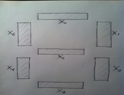
Another set up consisted of a circuit for 7-segemnt display with 3-bits; the A1, A2, and A3 to enable the inputs to display “UC DAIVS”. The order of output dedicated the use of 3 input NAND gates, 2 input NAND gates, and an inverter. A truth table was also used to calculate the 7’s outputs to provide the display due due to the 3-bit inputs.
The above display has 7 signal inputs. With a low (0) signal input, light shows, otherwise, not. We call it an “Active low” with low input voltage, but high output. Active low reduces leakage voltage and power resulting in noise than the active high.
The order of the inputs allow the display to light with a single letter “UC DAVIS”. For example, if inputs (A1, A2, A3) were 000, then all output displays could be low excluding the X0 output, hence displaying letter “U” with a blank line between “C” and “D”. All output X’s would be high and no light up. Further more, the truth table would help to generate the function of the diplay (Figure-2).
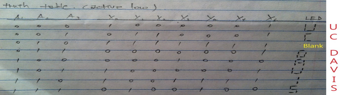
Following the truth table, each output display can be created in order to SOP, sum of product with the Kernel-map.
- X0 = ~A1ㆍ~A3 + A2ㆍ~A3 + A1ㆍ~A2ㆍA3
- X1 = ~A1ㆍ~A2ㆍA3 + ~A1ㆍA2ㆍ~A3 + A1ㆍA2ㆍA3
- X2 = ~A1ㆍ~A2ㆍA3 + ~A1ㆍA2ㆍ~A3
- X3 = A2ㆍ~A3 + A1ㆍ~A3
- X4 = A2ㆍ~A3 + A1ㆍA2ㆍA3
- X5 = A2ㆍ~A3
- X6 = ~A1 + A2ㆍ~A3 + ~A2ㆍA3
Using Bubble pushing theory, SOP is a 3 NAND gate. To verify the truth table and kernel map, a NAND gate was built with 5V with apower supply and an oscilloscope connected to the circuit board. Low output prompted input to be varied. Tests were conducted with the LED display, to calculate the value of the current limiting resistor. With a 5-voltage input and a continuous forward current per segment in the display of 30mA, the resistor used had a resistance of 166.67 Ohm.
NATCAR Design (DC Motor Control)
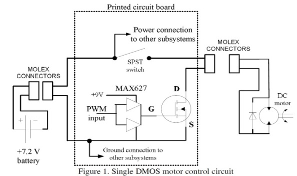
The DC motor control used in the NATCAR keeps the motor speed independent of feedback. The open loop system is controlled directly by the use of inputs from stereo volume control, which accelerates the electric drill. The experiment is based on Figure 1, a simple diagram of an open-loop DC motor control, which uses the generator to produce -13V sine wave input signal. MAX 627 IC gets the PWM signal as input and translates it into voltage/current output. The DMOs take output to control the speed of the motor depending on the output signal. In this setup, additional electric components were used. These included, a +9V switching regulator board with a +5V linear regulator, H-bridge PCB to protect the MAX 627 current overflow, DMOS heat sink to avoid overheating, and a 4WD car model (NATCAR with motor) soldered to the board. The function generator was used to produce 0-3V square wave with 5 KHz and a duty cycle of about 25% for the test. The oscilloscope settings were checked for an output of +7.2V from the battery and +9.0V for MAX 627 power. The speed was gradually controlled in order maintain a certain level of duty cycles on the generator by using the duty cycle knob to vary the value to vary between 10% and 90%.
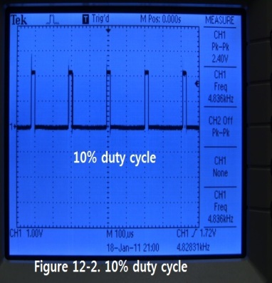
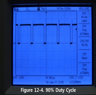
Results showed that the PWM signal on the oscilloscope varied the duty cycles so that the speed of the motor could be controlled using the signal. Higher duty circles resulted from higher values on the knob.
Works Cited
Ellersick, William F. “Data Converters for High Speed CMOS Links”. Computer Systems Laboratory Departments of Electrical Engineering & Computer Science. (2001). Web.
